Intro On How To Program Electronic Circuits In VHDL, and Why VHDL Is a Great Language!
Intro to VHDL Programming
I won’t bore you with the meaning of the “V.H.D.L.” name since you can find the meaning of its name anywhere on internet, but just know it is a fantastic means to describe digital circuits with nothing more than text.
Also remember that VHDL is a parallel programming code, and nothing like any other previous language code like Basic, Assembler, C#, C++ etc. Which in short means that your circuit Inputs, Outputs and inbetween transfers, all will be processed in the same time! And not like for instance in Basic Sequential, from top to program bottom, but instantly. And at unbelievable speeds way above 50 Mhz, and much faster as its Harvard structured and Von Neumann based Processors at equivalent speeds.
We call this way of programming and executing code in VHDL “Concurrent”. And because the FPGA/CPLD chips, where we program our resulting VHDL code into are also very fast, we are able to create any big software developed circuit into a small chip. Which also saves pcb size, space and also cuts down the power dissipation. (In the old days we needed a lot of TTL/CMOS digital chips on a very big board to accomplish the same task. But at much lower speeds and larger dissipating currents.)
What you also have to know furthermore is that every Manufacturer sells his own specific type of FPGA/CPLD Complex Logic devices, and also uses their own matching Development Program and special JTAG programming interface, and/or VHDL Development Board. Only the JTAG itself is kind of standard and just another interface connector to be able to Flash our FPGA chip. Which means that any FPGA chip can be seen in another Manufacturer’s Development Program by using his JTAG interface, but it still can’t program the chip from another Manufacturer. Therefore you need to use its matching Development JTAG interface AND matching Development software. Like the ICSP/ISP connector is for Arduino Boards. And the same goes for PIC microcontrollers which also have ISP connection interface Pins. But this also points out that Microcontrollers are sequentially programmed devices and unable to program by using VHDL code.
To name the three most well known FPGA/CPLD Manufacturers, we have Xilinx, Atmel and Altera. But there is also Lattice to just name another. Xilinx software can be ordered Free at no cost; Atmel and Altera require licenses and are only free for a limited (Trial) time. And there are also a few Free programming Tools from all of them but they have fewer possibilities. And VHDL circuits printed out on paper all look different compared to each other. JTAG interfaces can be found very cheap on Ebay for all Manufacturers, but for Atmel FPGA programming you have to buy theirs.
In our VHDL software development environment like in C we start by declaring the necessary VHDL IEEE libraries. But there any similarity with sequential programming languages like C ends.
Next I will show you how to program a Mux in VHDL code. Starting with the way how the digital circuit looks on component level.
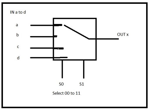
First I will present the picture of a Mux to explain what it does. We have 4 inputs a,b,c and d.
What input will be connected to output X depends on Selection Bits S0 and S1. If S0,S1 are “00” we have selected input a, up to “11” which represents input d.
All we now have to do is translate this into VHDL code. There are more ways to skin a cat in VHDL (to use an old expression). And all work!
First we need, as in any method is the same, to declare the IEEE VHDL libraries we will use, next we have to describe how the VHDL code has to communicate with our circuit by first describing its ENTITY.
That is quite easy as next code shows:
ENTITY mux IS
PORT (a, b, c, d : IN Bit;
s0, s1 : IN Bit;
X : OUT Bit);
END mux;
It in short explains to our VHDL Software where our PORT Inputs and Outputs are. However according to new IEEE 1164 rules instead of using BIT from the older IEEE 1076 VHDL library the newer STD_LOGIC_1164.all (as in Standard_Logic) is prefered. Although BIT probably still will work.
Now we continue with creating the ARCHITECTURE part which will describe how our in ENTITY described circuit will use these PORT signals. Because we upto now only explained the INs and OUTs of our circuit as being the unknown Black Box circuit. Also because we also can Simulate our circuit afterwards we have to add the Architecture to the Entity part.
Here we will use one of the possible Architecture statements:
ARCHITECTURE BEHAVIOR OF mux IS
SIGNAL select : INTEGER;
BEGIN
Select <= 0 WHEN s0 = ‘0’ AND s1 = ‘0’ ELSE 1 WHEN s0 =’1’ AND s1 = ‘0’ ELSE
2 WHEN s0 =’0’ AND s1 = ‘1’ ELSE 3;
` x <= a AFTER 0.5 nS WHEN select = 0 ELSE b AFTER 0.5 nS WHEN select = 1 ELSE
C AFTER 0.5 nS WHEN select = 2 ELSE d AFTER 0.5 nS;
END BEHAVIOR;
Although our above ARCHITECTURE (by using the Concurrent way) perfectly describes how our circuit operates function wise, it is just one of the different ways we can describe it.
Another way is writing it in the Sequential notation:
ARCHITECTURE sequential OF mux IS
(a,b,c,d, s0 , s1)
variable select : Integer;
BEGIN
IF s0 = ‘0’ and s1 = ‘0’ THEN select := 0;
ELSIF s0 = ‘1’ and s1 = ‘0’ THEN select := 1;
ELSIF s0 = ’0’and s1 = ‘1’ THEN select := 2;
ELSE select := 3;
END IF;
CASE select IS
WHEN 0 => x <= a;
WHEN 1 => x <= b;
WHEN 2 => x <= c;
WHEN OTHERS => x<=d;
END CASE;
END PROCESS;
END Sequential;
Previous VHDL code still looks a lot like the first program.
In the beginning I made the error to write ELSEIF instead of ELSIF, so watch for this mistake when writing your own VHDL code.
Because I still am an electronics engineer above ways are not my favorit ways. My favorit way of describing is the NETLIST way which is much more describing the circuit at component level. And therefore also better suited I think to describe any other circuit that needs to be translated into VHDL code. The NETLIST is simply said an easy way how to explain in VHDL how our gates are wired. It is probably however not very well suited when you are going to write very big circuits. In that cases you better write your code in one of the above ways presented.
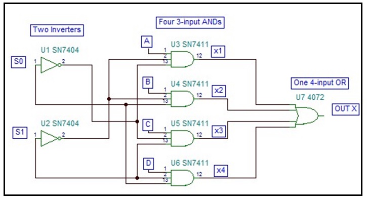
But before I can show the Netlist way, I first have to show our previous circuit in gate technology. With ANDs, ORs and so on.
And with this very clear circuit we have the same Mux but completely described in gate technology. It is easily showing that output AND U3 signal x1 which is input signal A, is selected when S0,S1 = ‘00’.
Now we are able to describe our ARCHITECTURE the NETLIST way:
ARCHITECTURE netlist of mux IS
COMPONENT ANDGATE
PORT (a,b,c,: IN BIT; X: OUT BIT); END COMPONENT;
COMPONENT ORGATE
PORT (a,b,c,d : IN BIT; X: OUT BIT); END COMPONENT;
COMPONENT INVERTER
PORT (inv : IN BIT; X : OUT BIT); END COMPONENT;
–This ends our gates port description how VHDL interfaces with our gates.
— Next in NETLIST part in our Architecture is description of how the components are wired together.
SIGNAL s0_inv, s1_inv, x1, x2, x3, x4 : BIT;
BEGIN
U1: INVERTER (s0, s0_inv);
U2: INVERTER (s1, s1_inv);
U3: ANDGATE (a, s0_inv, s1_inv, X1);
U4: ANDGATE (b, s0, s1_inv, X2);
U5: ANDGATE (c, s0_inv, s1, X3);
U6: ANDGATE (d, s0, s1_inv, X4);
U7: ORGATE ( x2 => b, x1=>a, X4=>d, X3=>c, X=>X );
END netlist;
It is easy to see how the last Architecture describes and exactly follows the connections from the Mux as created in the circuit on gate level. U1 to U7 represent all gates from the given circuit. I must make a note here that the VHDL code in this form will not work in all VHDL compilers. Because it didn’t work in this notation in Accolade’s PeakFPGA without a few changes, but probably will run perfectly in Model Technology Inc.’s Exemplar Logic Inc. synthesis tools. Also in PeakFPGA the compiler uses the STRUCTURE command to tell the VHDL program that it will be connecting wires (Signals) at low level GATE component structure.
All you now have to do after making this circuit in VHDL code, is test it in a VHDL Simulator. By making a testbench that simulates all possible inputs to check the created Output waves in a time or wave diagram.
I myself have the Free Symphony EDA Simili Simulator. Free License after registration for Limited Similator use, no saving WAVES, (no time limit), Atmel’s ProCHIP temporary Free Licensed (and PeakFPGA) , Xilinx Vivado DESIGN SUITE dvd (Free obtainable on-line – From Singapore distributed with FEDEX).
And there must be hundreds more that give plenty of learning and Simulating VHDL code possibilities. Like for instance the very good but also extremely buggy QUCS!
But instead of directly writing your circuits in VHDL you still can use programs like Protel 99, WinCupl or other VHDL designers to start by drawing your circuit and afterwards compiling it into VHDL code form. Although the above briefly mentioned QUCS is extremely Buggy , it really does do both !, including making a Testbench and a Wave diagram or Time diagram from your design under test. (DUT). So only while QUCS is very Buggy (it hangs its program in no time without giving any clue most of the time), it still would be the best program I ever encountered, because it also is capable of designing Digital and Analog circuits altogether ! And if the designers ever manage to remove the terrible bugs from Qucs they could have made the ultimate Circuit designer, VHDL creator, Simulator and Electronic circuit creator – all in one – worth buying! And Qucs is available in different versions, also known as QucsStudio, on the internet. 0.018 is the latest version but version 0.019 is in the making. And Qucs is also richly documented in several also free and very large PDF books. And it is available both for Windows and for other OS like Linux and Macbooks. But there are many more Electronics Circuit Designers that are capable of creating VHDL code like the Analog and Digital circuit Designer Tina. Although their VHDL module is probably still an option and would cost extra. Nevertheless it is affordable and also very useful for Engineers who want to simulate their circuit and afterwards want to create the PCB for it too. What in Tina also can be simulated and watched at every angle, even before actually building the Board.
Hope it was a brief but exiting intro into VHDL programming.


Tidak ada komentar: